


Description
Photolithography is an indispensable manufacturing process for modern computer chips and integrated circuits (ICs) and is undoubtedly one of the most important technologies of the current information age. However, this manufacturing process is not only suitable for producing silicon semiconductors but generally enables the fabrication of precise structures on a variety of materials. The goal of the research project "Scanning Beam Interference Lithography on Spatial Structures" is to develop methods for the efficient fabrication of optical grating structures on curved surfaces. The method used for structuring, Scanning Beam Interference Lithography (SBIL), is ideally suited for creating fine gratings over a large working area comparatively quickly and has already been proven for planar gratings. However, the planned flexibility to also produce non-planar grating structures would open up many new areas of application, particularly in the fabrication of diffractive optical elements, which are extremely relevant for laser optics, for example.
The 3D-SBIL Writing Head
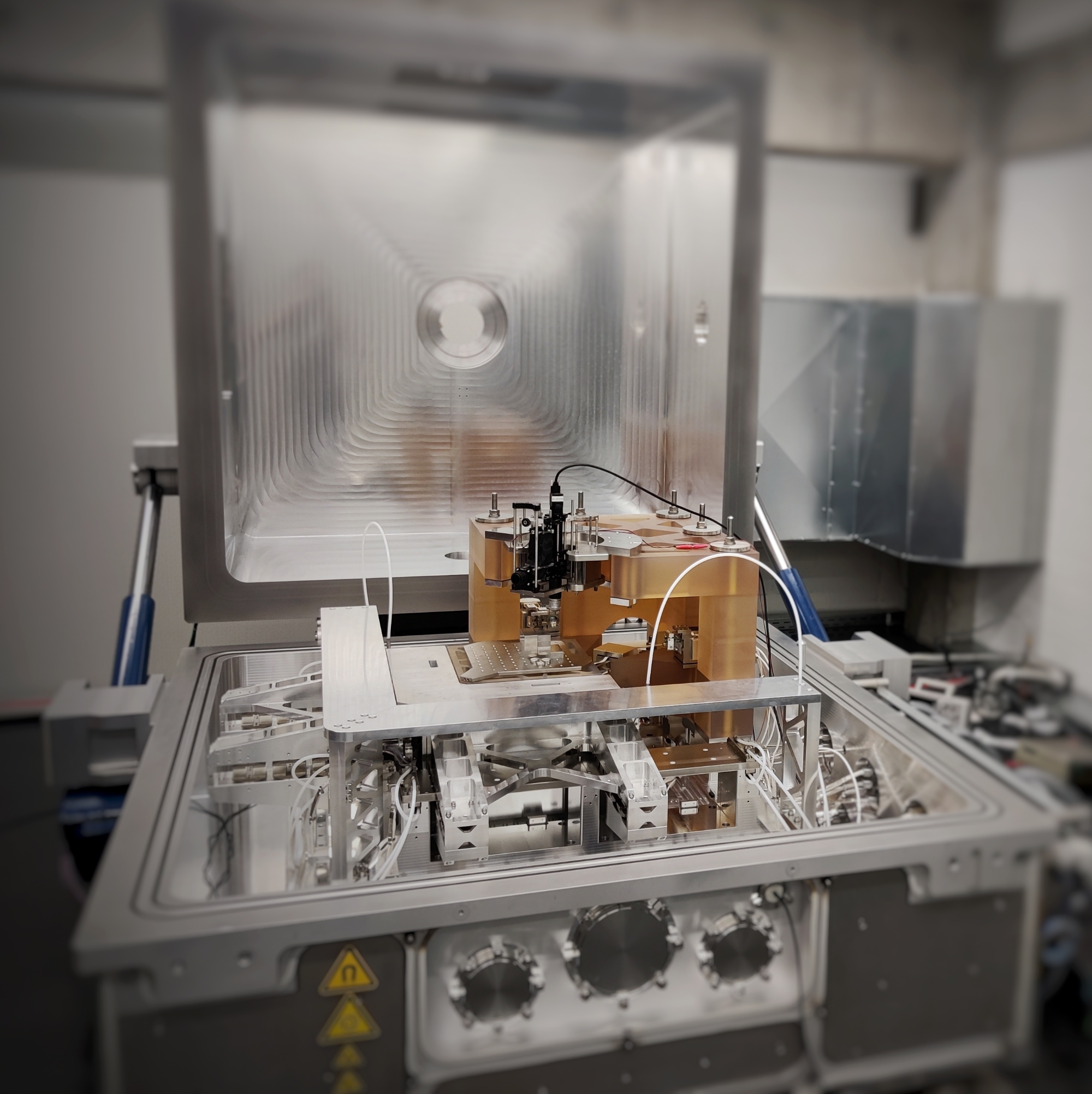
The central element is a novel writing head that dynamically adapts the interference pattern to the local topography of the substrate. It possesses five mechanical degrees of freedom (5-DOF) to actively control the grating period, rotation, and inclination (tip/tilt) of the writing spot during the process. This enables precise alignment of the writing beam even on complexly shaped surfaces.

High-Precision Positioning with the NPMM-200
To ensure the required positioning accuracy in the nanometer range over a large working area of 200 × 200 mm, the writing head is rigidly mounted above a Nanopositioning and Nanomeasuring Machine (NPMM-200). This machine features a measurement resolution of 20 pm, enabling path deviations in the double-digit nanometer range.
Partners
Current partner:
- Institute of Process Measurement and Sensor Technology (IPMS)
- Institute of Applied Optics (ITO)
Funding
This project is funded by the German Research Foundation (DFG).
Coordinator

Josias Rühle
M.Sc.Research Assistant